The demand for ever-increasing functionality in smart devices is driving up silicon chip complexity, which is at the heart of these systems. To compound the challenge for chip designers, consumers are demanding more performance per watt to improve the battery life and sustainability of their products.
Chip Design Challenges
These needs are driving the move to smaller and smaller technology nodes, with some of the most advanced silicon at sub-10nm today. And, of course, all of these requirements must be met despite shrinking development schedules and modest (if any) increases in available resources and headcount.
Consequently, chip developers must do an increasing amount of design simulation and analysis under very tight schedules before tape-out and release to manufacturing.
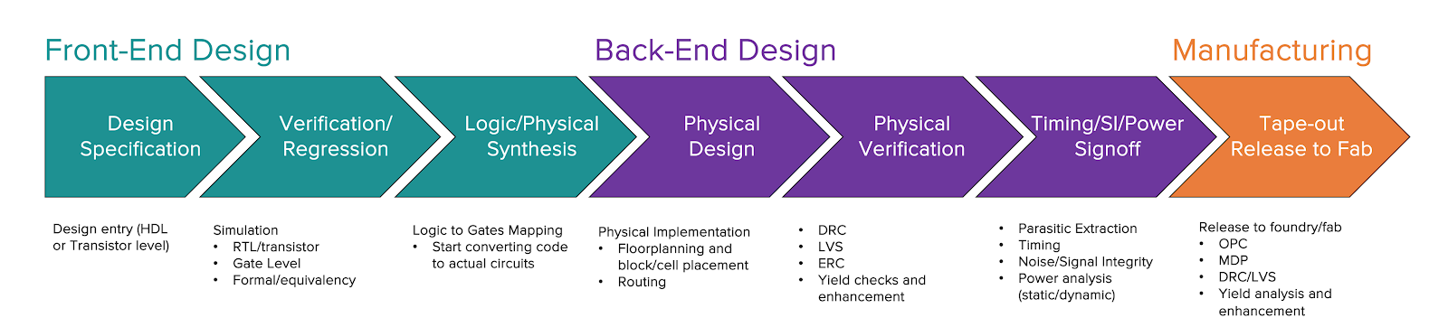
The chip design workflow shown below illustrates the major phases of the development process. Some of the major challenges that electronic design automation (EDA) designers face today include:
- More complexity › higher transistor and gate counts
- Better power management › more power modes and more complex analyses needed
- Advanced technology nodes › more complex simulation requirements and additional modes and corners to take into account
These trends come hand in hand with a huge increase in data volume. The increased data volume has significant implications. In fact, I/O performance can have a huge impact on EDA job performance throughout the chip design workflow. It all points to the need for very careful data management.
To illustrate the impact of these challenges, I recommend taking a look at this excellent paper by Intel. Intel clearly is in the forefront of cutting edge technology, and they have published their own datacenter utilization and growth statistics to support their latest design projects.
I have reproduced one of their interesting graphs here. What they show is a 30+% CAGR of compute and storage over the last 10 years, with no abatement in site.
While Intel may be somewhat of a special case in EDA, we hear from many of our customers that they fall into the 20+% annual growth rate. Sometimes they do see “quantum jumps,” especially when they migrate to advanced technology nodes or start big designs.
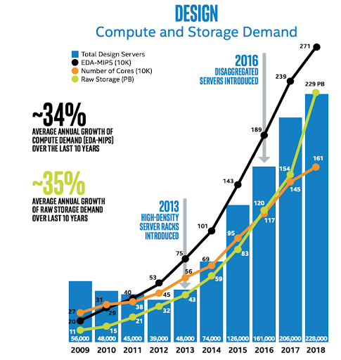
Source: Intel
Measuring I/O Impact
Software builds are a huge component of modern chip development and are a good example of the I/O challenges.
A good way to measure I/O or storage impact is by looking at CPU vs Wall-clock time of a job. (Here’s a refresher on the time command.)
For example, we ran an experiment in our labs and a single software build of OpenSSL over the NFS protocol on shared storage systems (prevalent and necessary in EDA environments) shows a real versus user time impact of 36%, which generally means the process time was impacted by 36%. The biggest bottleneck: Waiting for I/O.
While some of this is unavoidable due to protocol or network overhead, we should strive to minimize the impact due to storage inefficiencies as much as possible.
Some organizations measure storage impact using a particular software build time (for example, the Linux kernel) as a “canary-in-the-coal-mine” indicator. They have measured the run time under various conditions and know that something is wrong when they see variances . Very clever!
We strongly encourage instrumenting your flows to determine how much you are being impacted.
Parallelism and Concurrency
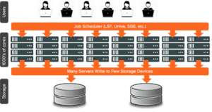
When many jobs run in parallel — the normal mode of operation in chip development environments which may have thousands of computational cores — traditional storage can often significantly cause a bottleneck and have a huge impact on job throughput and performance.
One of the causes is that many clients are reading and writing data at the same time. Traditional storage can quickly run out of system resources under this scenario and can significantly slow down and cause queuing.
An interesting aspect of this phenomenon is that many users don’t even realize it is happening… How often have you heard this lament, “My regression always takes 7 hours”? In fact, it could be a lot faster.
Customers tell us many jobs fall into this class of high concurrency and parallelism, including (but not limited to) RTL simulation, software design, physical design, physical verification, timing, and tapeout.
Pure Storage FlashBlade™ is in a unique position to help address the challenges of increasing design complexity and the need to handle very high levels of concurrency and parallelism. FlashBlade is optimized to handle high client counts and scale linearly.
EDA and software workloads also tend to have very unique storage I/O characteristics — they tend to be metadata dominant — which is a particular sweet spot for the FlashBlade architecture.
As an example of workload characteristics, take a look at the following RPC profile from one of our semiconductor customers’ storage arrays running front and back end design flows. If you sum up the metadata calls — including GETATTR, ACCESS and LOOKUP — you can see they make up more than 85% of all the NFS calls received by this array over the monitoring window, while Read and Write are less than 15%.

Parallel Kernel Builds

A good test for evaluating metadata performance is running many software builds in parallel. What makes this experiment particularly useful is that it doesn’t require tying up expensive EDA licenses and it can be run relatively simply. It is also a good representation of EDA workloads in that it is a metadata-heavy workload (80+%).
As an example of how FlashBlade behaves for metadata intensive workloads, we ran a test case of up to 100 parallel builds of the Linux kernel in our lab (with 6 threads per build) and saw almost no impact in average build time when running a small FlashBlade system.
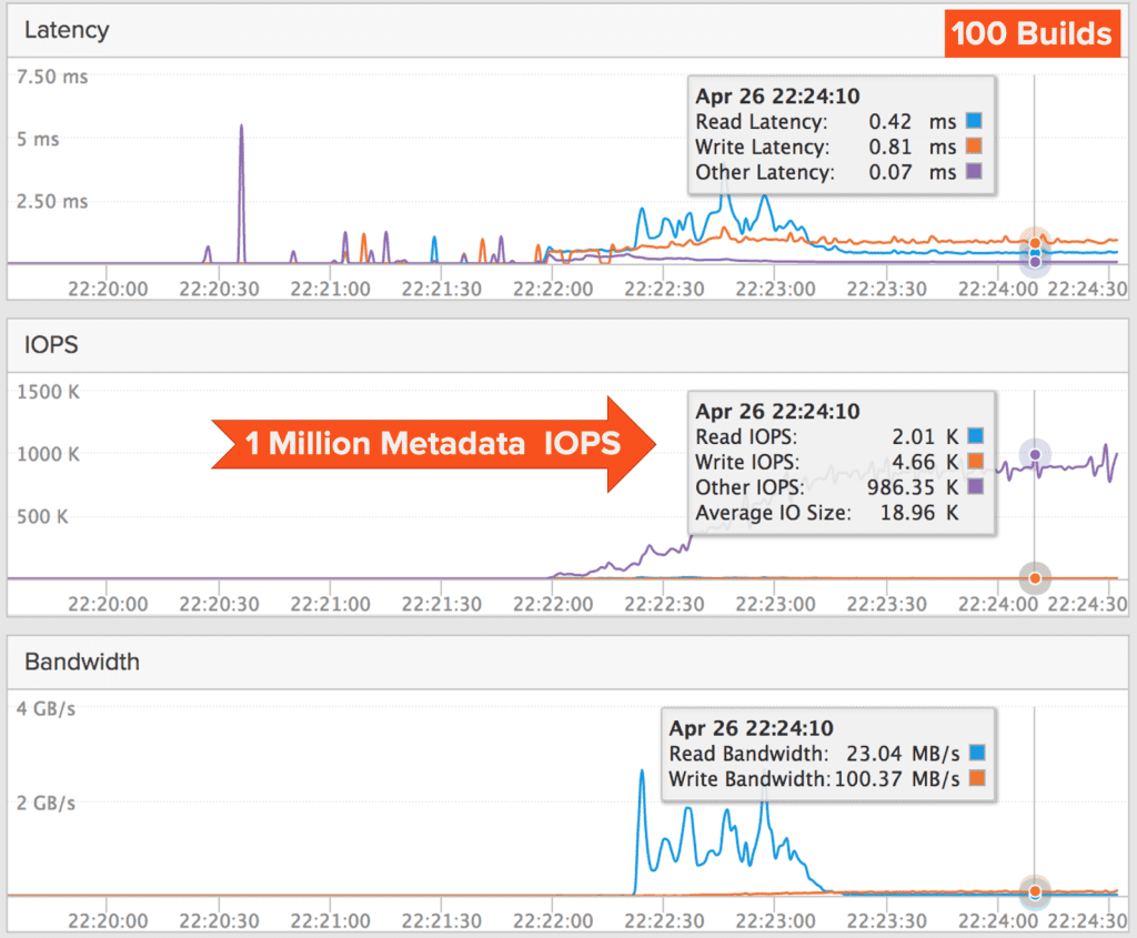
Actually, we did see a fall off at 100 builds. But that was because we had run out of cores and were oversubscribing the CPUs in our compute farm. (We only had 500 cores in our test bed, but 600 were needed.) However, in this test, we did achieve ~1 million NFS IOPS (as shown in the graph below.
Are You Impacted?
As I’ve illustrated, storage can have a major impact on EDA flows and overall productivity in chip design environments. Are you impacted? To see where your systems stand, I highly recommend running the above some experiments to find out.
If you find that faster I/O might benefit you, read part 2 of this series to learn the huge impact FlashBlade is making in the semiconductor industry.
Written By: