Semiconductor chips are at the heart of all the smart devices that we use every day. There’s an ever-increasing demand from consumers for products that are faster, cheaper, smaller, and have longer battery life. All these requirements are pushing chip designers to pack more functionality into silicon and move to more advanced technology nodes to manage power and costs. These changes in turn lead to huge increases in product complexity, which then increase the amount of analysis required before tapeout. To compound the challenges, all these requirements must be met in shrinking development schedules with a modest (if any) increase in available resources and headcount. Here, we will teach you how to scale EDA workloads with FlashBlade all-flash storage.
For a deep dive into this subject, I invite you to visit my blog series,”Real-world File Storage Performance with FlashBlade in Chip Design.”
Highly Parallel and Concurrent Workloads
Electronic Design Automation (EDA) development environments tend to have very high levels of concurrency and parallelism. Compute environments often have 10s-100s of thousands of cores, with many jobs accessing the same project folders and performing huge amounts of concurrent I/O operations. In these circumstances, storage can often become a performance bottleneck with significant impact to EDA job run times.
A critical capability of storage in EDA and high-performance computing environments is the ability to scale storage performance linearly as needed to mitigate the effect of storage-related slowdowns. In our labs, we ran some performance scalability tests that highlight the unique capabilities of FlashBlade® in this area.
Workloads Tested
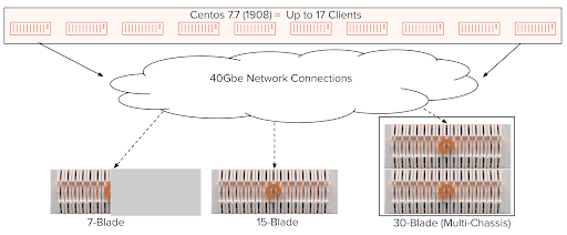
For this evaluation, we ran multiple workloads at scale against several FlashBlade configurations. We ran the workloads on up to 17 servers and measured the performance of 7-, 15-, and 30-blade configurations. The compute nodes were connected with a 40Gbps network.
The EDA workload profiles were generated based on RPC analysis and input from existing Pure Storage® customers. These represent major phases in the chip development process.
| Profile | Description |
| Read-only | Metadata-only workload representing read-only EDA workloads found for serving reference libraries, source code, etc. |
99% Metadata
Front-end Design (FE)Workload representing front-end EDA workloads (e.g., logic simulation and regressions).
85% Metadata, 15% R/W
Front-end + Back-end
Design (EDA Mixed)
Workload representing front- and back-end EDA workloads (e.g., logic sim, regression, physical design, signoff, physical verification, tapeout).
55% Metadata, 45% R/W
The Data Center of the Future Is All-flash. Will the Last HDD Seller Please Turn Out the Lights?
Results
In general, we saw excellent performance scaling in both IOPs and bandwidth as we increased the number of blades in the FlashBlade configuration. As you can see in the results graphs below, performance scaled extremely well as we increased blade count. All the results show performance relative to a seven-blade system. FlashBlade easily scaled in the multi-million IOPs range and reached multiple gigabytes per second of bandwidth during these tests.
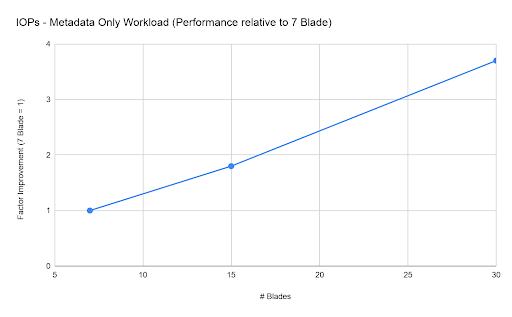
The metadata-only results just show IOPs performance since that was the dominant factor in this profile. As you can see in the graph below, we experienced almost perfect scaling on IOPs as we increased the configuration from seven to 30 blades.
The front-end workload which was 85% metadata and 15% R/W also scaled very well, with bandwidth actually scaling at a superlinear rate. The FlashBlade architecture allows for very efficient handling of compressible data which can contribute to excellent throughput performance. The data that was generated for this test had a compression ratio of 1.3:1, which is more conservative than what we generally see for EDA environments.
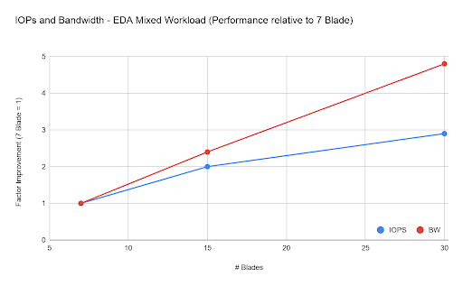
We see similar scaling behavior with the EDA-mixed workload, which had a high percentage of large file I/O (55% metadata, 45% R/W).
Takeaways
All the various EDA-workload mixes demonstrated excellent performance scaling for both metadata and IOPs when we increased blade count.
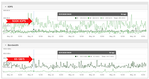
EDA workloads are known to be metadata intensive in the front-end part of the design cycle, but for advanced node designs, we are also seeing massive increases in throughput requirements for the back-end phase. The figure below shows the performance of a 75-blade FlashBlade in production that one of our customers deployed for physical design and signoff at sub-10nm, and it’s achieving 65GB/s and 500-700K IOPs. The ability of FlashBlade to serve both high bandwidth and IOPs at the same time is another unique capability of the architecture.
This kind of multidimensional scaling performance is exactly what is needed by semiconductor design companies as they continually innovate new products which require huge increases in compute capacity and I/O performance.
FlashBlade delivers a unique architecture in which increasing performance and capacity is simply a case of adding more blades into a cluster very quickly without any downtime, interruption of service, or data migrations. FlashBlade clusters are able to scale to 150 blades and 9PB effective in one namespace, giving users the performance and capacity scaling that are critical for next-generation semiconductor designs.