Summary
Learn the engineering advancements of Pure Storage’s FlashArray//X, focusing on its DirectFlash™ technology and NVMe architecture to deliver exceptional performance, efficiency, and scalability for modern data workloads.
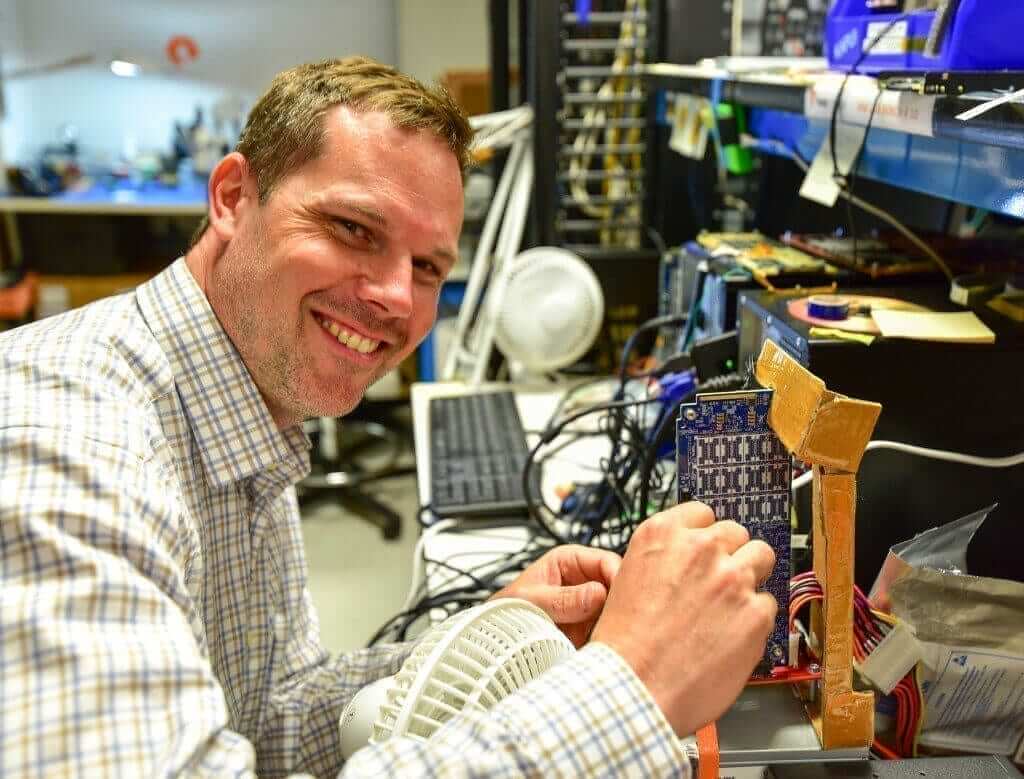
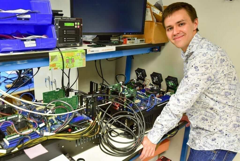
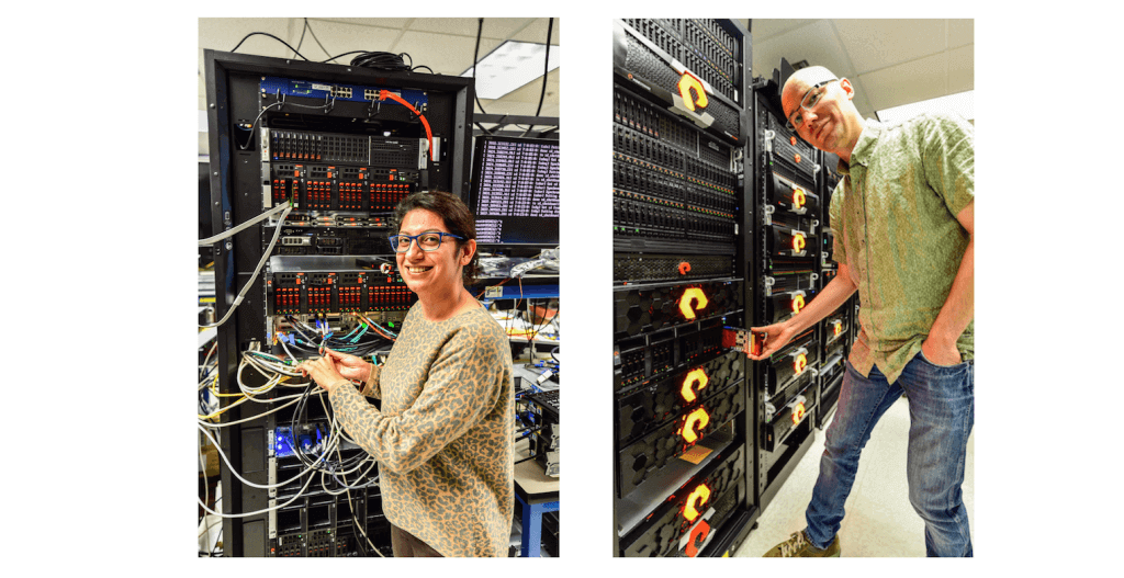
In this article, I would like to give you an engineer’s view of the Pure Storage FlashArray//X. We think we’ve built something special, and we hope our customers will be pleased with the results of our work.
When I first started at Pure Storage, everyone was excited by the performance of flash. But even back then, the architects of the Purity Operating Environment software were aware of the limitations of the SSD architecture and were making plans for the future.
With FlashArray//X, we designed a new storage architecture that allows us to improve our capabilities in many dimensions at once: performance, density, efficiency, and supportability.

Some FlashArray History
512-byte sectors have a respectable 30+ year history, but there comes a time when emulating ancient hard disk interfaces becomes a limitation. Modern flash uses 8-16MB physical blocks; commodity SSDs are forced to make compromises in order to emulate 512-byte (or 4096-byte) sectors on flash– data needs to be copied around to free up space to allow the large physical blocks to be reclaimed, erased, and reused.
The resulting Flash Translation Layer (FTL) software resides in the firmware of every SSD. The FTL implements clever garbage collection (GC) algorithms to copy data around and provide the illusion of a small logical sector. The costs of the FTL add up quickly, however: performance (both throughput and latency) can become unpredictable, and wear can accelerate due to subtle workload characteristics.
Since announcing FlashArray in 2011, we’ve managed SSD performance and lifespan with our Flash Personality Layer, which models the internal behavior of individual SSDs and optimizes Purity’s I/O behavior to get the best performance from every SSD in our flash modules. But we’ve always fantasized about a flash module architecture that wouldn’t require so much tuning; one that would simply get out of the way and let us use the flash in the most efficient way possible. So we finally decided to build one.
A New Flash I/O Architecture
There was a hidden potential within every FlashArray//M chassis, since the first one we shipped: an NVMe link between the controllers and the flash module bays. While we were busy designing NVMe NVRAM modules, we were daydreaming about the flash modules we would get to build next.
NVMe is a great protocol: it’s lightweight, powerful, easy to use, and easily takes advantage of highly multi-core processors. Just switching to NVMe alone would provide a nice performance boost, but we wanted to go further—a lot further.
“Throw out the FTL” may not sound like much of a plan, but it was the core idea that led to the FlashArray//X DirectFlashTM Modules. If we could get rid of the SSD-based FTL and firmware GC, we could see dramatic improvements in performance. Every read or write performed could do the minimum possible work, never held back by a traffic jam of GC data migrations, busy flash dies, or complicated caching semantics.
We also invented new ways of sharing the flash management tasks between firmware code running inside the module’s embedded processors and the Purity code running inside the FlashArray//X Xeon processors. This will allow us to come up with new flash module innovations while maintaining compatibility with today’s software. And each new generation of software can redefine how the flash should be used.
DirectFlash Performance
DirectFlash Modules are dual-ported NVMe devices. Each has ~2GBps of raw bandwidth to each controller, enough to enable performance growth for years to come.
Each module can handle large numbers of commands in parallel; one per flash die (and just one 9.1TB module contains 256 dies). The combination of a lightweight protocol, massive parallelism, and high bandwidth means we can pack more performance into a smaller package than ever before.

It’s also nice to wave goodbye to the complex SCSI stack (another 30-year-old standard), the often-incompatible SATA command set, and SAT interposers that try to bridge the gap. NVMe allows software and flash modules to speak the same language. In addition, NVMe is designed to work efficiently on today’s multi-core CPUs, allowing every thread to issue I/O in a lock-free, cache-friendly way.
Even more interesting than the raw throughput is the fact that there are no qualifications on that performance. When the DirectFlash module is 100% full it will have exactly the same read and write performance characteristics (latency and throughput) as when it was new. There are no “special” workloads that can push its performance into unusual corner cases.
This is a big step forward over conventional SSDs which are very hard to manage and predict. Read and write latencies can sometimes jump by a factor of 100 depending on workload, drive fullness and history (yesterday’s write patterns can affect today’s performance).
Smart Endurance
Absolute performance is great, but as an engineer it’s incredibly satisfying to know that we’re taking all of our hardware resources and putting them to good use, with no waste, bottlenecks, or mismatched design priorities.
DirectFlash Modules add no write amplification. Purity manages data at the granularity of flash blocks, so there is no module-level garbage collection at all. We expect that this should double the flash lifespan.
Additionally, DirectFlash Modules have no over-provisioning. All the physical flash is visible to Purity software at all times. Purity does consume some of that space for RAID-HA, metadata, and other purposes, but at the end of the day there is still significantly more flash put to work for customers.

This is possible because Purity is able to manage data at the granularity of flash blocks. This is a nice benefit of having built a flash-friendly design over the last 6 years. Purity stores data in segments that span multiple devices, but are always one allocation unit in “height.” The Purity allocation unit now follows the flash block size, meaning when a segment is retired there is no more work to be done; all the segment’s blocks are immediately ready for re-use.
Adaptive I/O Control
Our DirectFlash Module has no logical address abstraction, which means that Purity is able to maintain perfect visibility into every I/O. We know which flash channel, die, and block is in use for every byte of data. This allows us to fine-tune our performance to a degree never possible before.
Because there is no garbage collection inside the flash module, there are no surprises. Purity I/O goes straight to flash. As a result the I/O latency to each module becomes effectively deterministic.
Existing Purity code already knows how to handle repair or migration of data, so we were able to manage new tasks like active wear leveling and bad block repair within the same code that performs all other reads and writes. Not only do we get the benefit of reusing well-tested software, but we also follow the same scheduling rules for best system performance.
Pure Simplicity
Our obsession with simplicity goes all the way through our product. We didn’t just do away with the SSD FTL; we also got rid of volatile write caches, complex metadata journaling schemes, and the need for hardware power-loss protection in every SSD. Because we control the location of every byte written, we know exactly when data has become non-volatile.
Like the array as a whole, the DirectFlash Module doesn’t have a shutdown procedure– just shut off the power (or yank out the module). We designed our flash-level metadata to be ridiculously simple: all metadata resides in the flash blocks alongside the data. This means that a power interruption is quite boring (no exciting rarely-used code paths)—the array simply resumes right where it left off.
Because the entire design (from hardware to software, kernel to cloud) is all created within the same team, all the pieces of FlashArray//X are designed to work together. To ensure everything meets the quality expected of a Pure product, our test automation simulates every failure we can think of– from a bad flash block to a kernel panic, many times per day.
And the day the product ships our job isn’t done: the FlashArray//X provides phone-home telemetry all the way down to the flash block level. In Pure1 we can monitor a wide range of flash characteristics, from wear distribution to block failures. Any anomalies can be investigated before they can cause customer-visible problems.

FlashArray//X continues to be an exciting project to work on; I can’t wait to see what customers do with it next. We promise we won’t stop thinking of more ways to improve what we ship every day.

Built to Scale
with Evergreen
See how Evergreen and Pure Storage simplify
storage management across any environment.
Latest Advancements in FlashArray//X: Pushing the Boundaries of Performance
Pure has continued to evolve the platform to meet the growing demands of modern data workloads. Below are the most recent updates and advancements in the FlashArray//X series:
1. Enhanced Performance with FlashArray//X R4
- The latest generation, FlashArray//X R4, delivers up to 40% more performance compared to its predecessors, ensuring faster data access for mission-critical workloads.
- Increased Memory Speeds: The R4 model features memory speeds improved by over 80%, enabling faster processing and reduced latency for high-demand applications.
- NVMe Everywhere: The system is built with end-to-end NVMe architecture, offering consistent low-latency performance, essential for real-time analytics, AI/ML workloads, and transactional databases.
2. Unified Block and File Storage
- FlashArray//X now integrates Unified Block and File Storage capabilities, eliminating the need for separate storage solutions. This unification simplifies infrastructure, reduces costs, and enhances data accessibility for both structured and unstructured workloads.
3. Evergreen Subscription Model
- The Evergreen//One subscription model allows organizations to future-proof their storage investments by providing non-disruptive hardware and software upgrades. Customers can seamlessly adopt new technologies without downtime or forklift upgrades.
4. Energy Efficiency and Sustainability
- The FlashArray//X series is designed with sustainability in mind, featuring energy-efficient technologies that reduce power and cooling requirements. This helps organizations lower their carbon footprint while maintaining top-tier performance.
5. AI-Driven Monitoring and Management with Pure1®
- With Pure1®, customers benefit from AI-driven predictive analytics and proactive support. Features like the Workload Planner enable organizations to simulate the impact of new applications or changes, ensuring optimal resource utilization.
6. Key Use Cases
- Database Optimization: Achieve lightning-fast performance for Oracle, SQL Server, and SAP HANA, with built-in tools for database protection and recovery.
- Virtualization: FlashArray//X continues to enhance virtualized environments with integrations like VMware vSphere, ensuring high availability and consistent performance.
- AI/ML Workloads: Its NVMe-driven architecture supports the high-throughput and low-latency demands of AI and machine learning applications.
7. Future-Ready Storage
- FlashArray//X is designed to handle the evolving demands of modern businesses, providing the scalability, reliability, and performance necessary for next-generation workloads.
By continuously innovating and refining FlashArray//X, Pure Storage ensures that organizations can confidently tackle their most demanding storage challenges while preparing for future growth and technological advancements.

Free Test Drive
Try FlashArray
Explore our unified block and file storage platform.


