
Summary
EDA design strains traditional data center infrastructure. With AI modeling, it’s become even more challenging. Pure Storage delivers the performance and flexibility EDA manufacturers require.
Summary
EDA design strains traditional data center infrastructure. With AI modeling, it’s become even more challenging. Pure Storage delivers the performance and flexibility EDA manufacturers require.


Industry demand and ubiquitous access to chip design tools has caused a resurgence in very large-scale integration (VLSI) designs and smarter electronic design automation (EDA) tools. Hyperscale cloud providers like Amazon, Google, and Microsoft—along with consumer computing companies like Apple—are heavily focused on building proprietary processor designs specific to their needs, while other manufacturers like Intel, AMD, and Qualcomm are all focusing on delivering sub-10 nm Application Specific Integrated Circuits (ASICs). These companies may all benefit from designing and building custom processors, but they also can struggle with the complexity, demands, and infrastructure strain that EDA design can put on IT operations.
In particular, current data centers may not be architected to support what EDA workflows demand from IT infrastructure—especially as generative AI modeling joins the fold to enhance and streamline the design and testing processes:
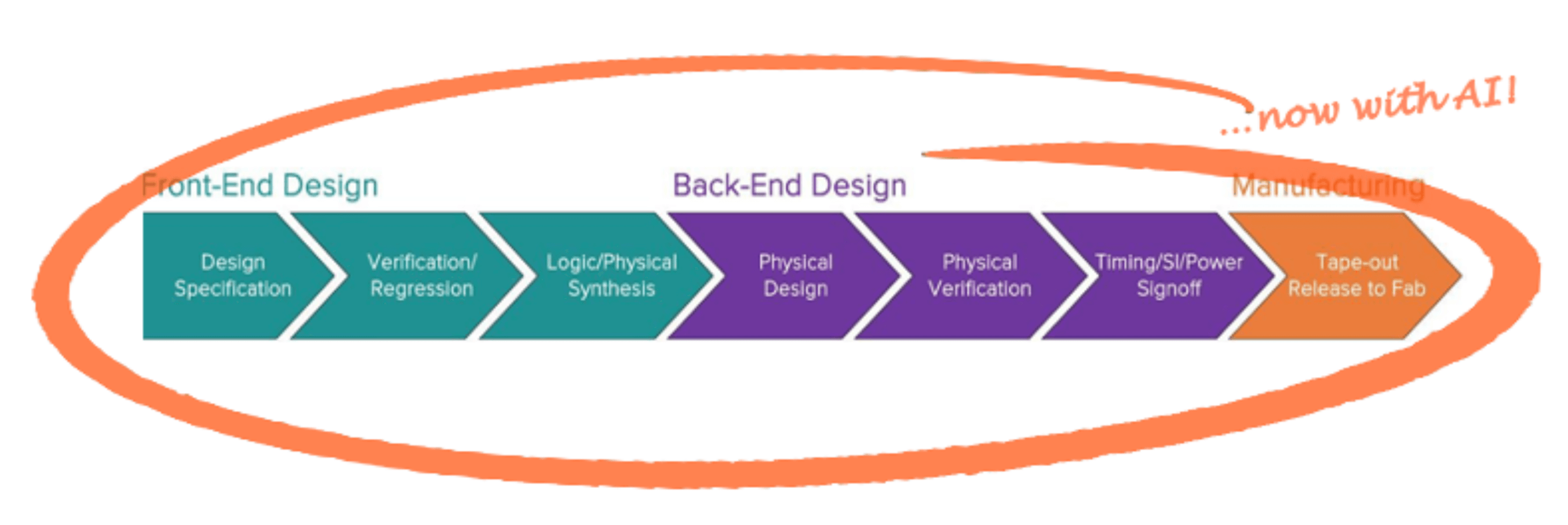
This introduces a new trade-off: AI’s inclusion can streamline and speed up a design’s release to manufacturing, but only if there are adequate compute, memory, and enterprise storage resources to scale and support it. In short, faster time-to-market comes at a price.
Setting Direction for Enterprise AI Infrastructure
Operational Efficiency Is Key to Faster Time-to-Market
The EDA and software design industries have one big thing in common: Speed of execution is a major competitive advantage. Time, as they say, is money. But workflows can only execute as well as the underlying data center infrastructure can support. Data center operation is designed to support EDA workflows with three “legs” of a stool:
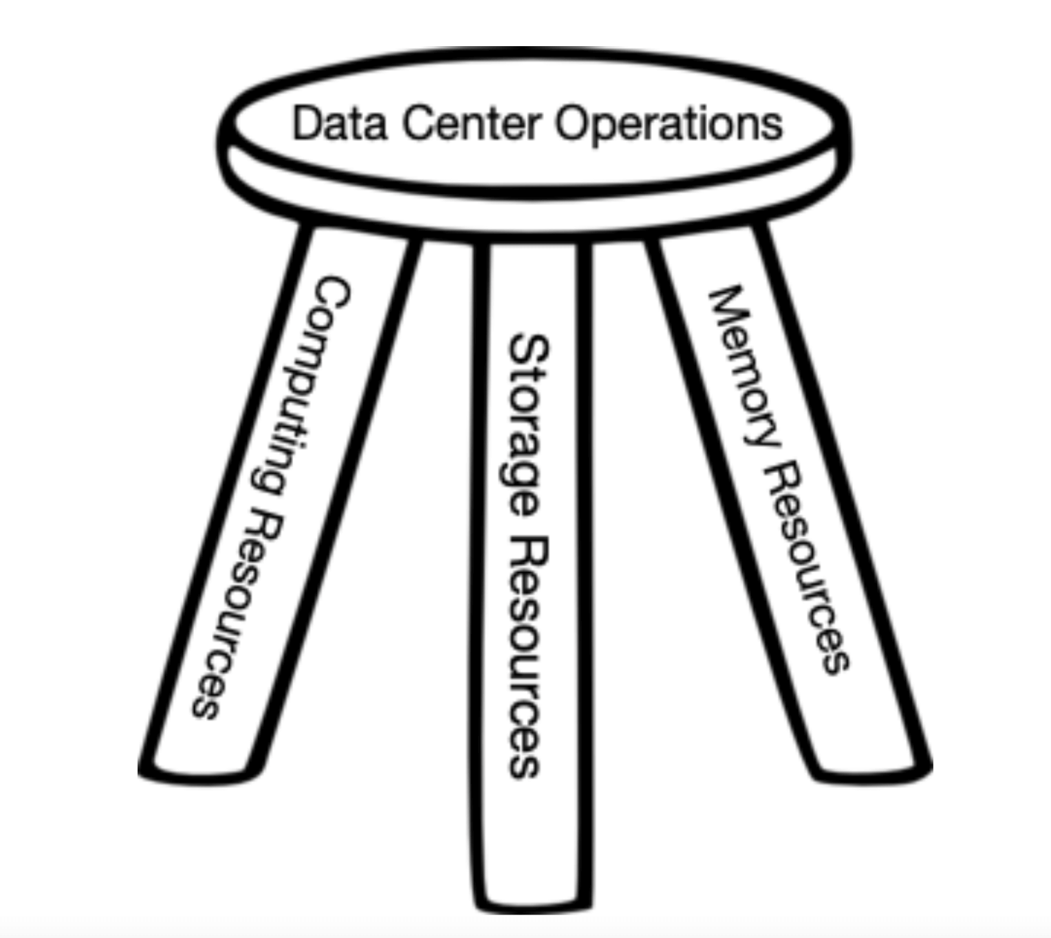
A complementary balance between these three elements is critical for an optimal EDA workflow execution that varies in its consumption. Bottlenecks in any leg of the stool will throw off the balance, slowing the whole process down and making the final design more expensive.
Data center technologies have to be flexible in their capabilities to maintain performance synchronicity. Add in generative AI for design optimization and it gets even more challenging:
- AI-augmented EDA workflows require variable storage performance needs during design verification. Oversubscribed storage causes unwanted delays in supporting requirements slowing the dev process.
- AI-based operations and high GPU usage result in increased data center footprint and high power draws. This means higher costs for rack space overages with potential service outages.
- AI-based workflows push the limits of traditional data center infrastructure designs. Legacy was not designed for the dynamic workloads of the AI-driven world we live in today.
Of the three legs of the stool, data storage has traditionally been the most inflexible. That’s because many array technologies currently sold by legacy vendors were designed decades ago when these dynamic workloads were less prevalent in mainstream computing.
Modern data platforms like Pure Storage, however, are purpose-built for agile enterprises and dynamic, demanding workloads. EDA designers no longer have to struggle to maintain balance and performance to produce results, and the ripple effects on the industry could be huge.
Accelerating Semiconductor Design Pipelines with Pure Storage FlashBlade//S
Pure Storage FlashBlade: The Flexible Data Array Made for EDA Manufacturers
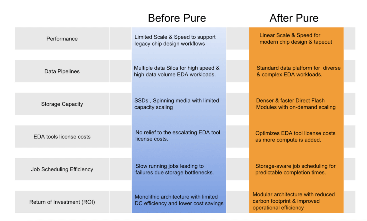
Pure Storage® FlashBlade//S™ combines scale-out, blade-based storage processing with a blend of NVMe and QLC-based flash memory, which enables up to two times more predictable and consistent performance improvement compared to our competitors’ storage arrays.
FlashBlade’s architecture accelerates everything in the EDA workflow: time-to-design, time-to-test, time-to-market, while at the lowest energy cost per TB in the industry. Its storage-aware job scheduling is transparent and uses simple storage APIs to avoid job failures. This also makes it easier to manage storage resources, greatly reducing the risk of enterprise storage being the production bottleneck.
More robust data protection and global collaboration are also possible with FlashBlade – immutable snapshots and asynchronous replication are built in with no need to employ additional technologies to achieve business goals and support a global workforce.
Pure Storage customers who have implemented FlashBlade® to support their production workflows have seen a significant improvement in their design outcomes:
Here’s another way to think about it:
Faster builds and regressions mean a quicker time-to-value for new chip designs, which means more predictable results that improve AI workflow times and capabilities. These savings can then be reinvested into other data center elements adding CPUs and GPUs for a more capable Silicon Life Cycle (SLC).
That’s not just a walk off home run, but a walk off GRAND SLAM!
Join Us at DAC 2024!
Be sure to register for the upcoming 2024 Design Automation Conference at the Moscone West conference center 06/23 – 06/27 and stop by booth 1315 to catch up with Pure Storage on how our data storage platform is a great investment for your EDA workflows!
Learn more about why Pure Storage is the best data platform for EDA manufacturers.
Check out this blog to learn more about EDA challanges and how to overcome them.

Written By:
Solve EDA Challenges
Learn what EDA is, why it’s important, what challenges EDA-based semiconductor chip manufacturers face.


