Listen to Better Science from the author himself, Justin Emerson!
Flash memory is pretty incredible stuff. At Pure Storage®, we’ve built our entire storage hardware portfolio on solid-state storage. We’ve eschewed disk as a relic of the past and are building a new generation of storage platforms centered around flash memory. We think storage is an industry still ripe for innovation, not commoditization.
But the incredible march of progress that has driven flash densities higher and higher is also slowly chipping away at its core purpose: to reliably store bits. Like a tragic superhero, its power for good is slowly killing it.
There’s good news: These are solvable problems, but they require new approaches to building systems that fundamentally reimagine how flash is managed. Let’s take a step back and look at how we got here. To do that, let’s talk about physics.
Learn how the all-flash data center is imminent
The Physics Behind Flash
Let’s start with how flash storage is built. Flash memory is a transistor—only, it’s a very special kind of transistor. If you put a voltage across the transistor, you want the electrons to flow, or not to flow across a gate. Using some pretty amazing physics, flash memory traps electrons inside this gate, which is measurable as a difference in voltage across the circuit, even after we cut power to the system.
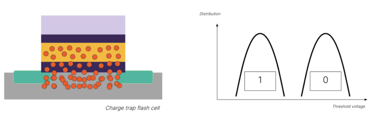
Why is this significant? We’ve now got a transistor that can store a bit, even after it’s been turned off!
Once we got the hang of this, we started to ask: “If we can measure that there are no electrons in the trap versus that there are electrons in the trap, what if we could measure some electrons? What about a few electrons?”

Now you’ve gone from storing one bit per cell (SLC) to two bits per cell (MLC). Congratulations! You’ve just doubled the density of every single transistor. It takes a bit more fancy signal processing, but you can measure four different voltage states to determine two bits. As time went on, we were able to discern three bits (TLC) and then four bits (QLC):

Now, we’re measuring 16 different possible voltage levels to store four bits. We’ve doubled the bits per cell from MLC, but we’ve quadrupled the number of voltage levels we have to discriminate between. Once we build these transistors, we pack as many of them as we can onto the most state-of-the-art semiconductor fabrication process, and then stack them into apartment building-like structures to store millions of bits:
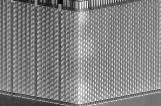
Kioxia 3D BICS NAND
Then, we take those structures and stack them on top of each other in multiple layers:
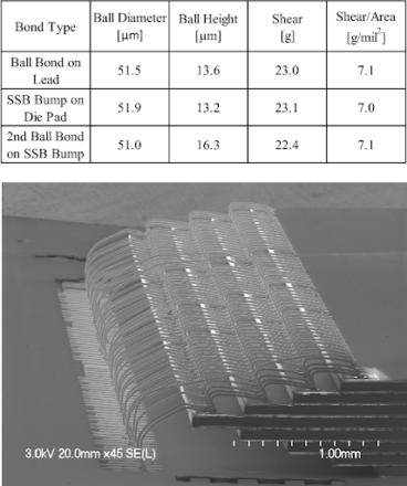
With these structures, we can store trillions (10^12) of bits on microchips the size of a coin. When you assemble these into full-fledged systems, you can store quadrillions (10^15) of bits in a single namespace.
Fill a data center with these and you’ve got yourself petabytes of all-flash storage. Pretty incredible stuff, right?
The Faustian Bargain
All of this density comes at a cost. Measuring different voltage levels may sound easy (even though we use the most advanced signal processing—the same kind we use to talk to spacecraft millions of miles away), the reality is that it doesn’t look like this:

Instead, each of these voltages is a probability distribution. As the bits get more and more packed, they begin to overlap:

The overlapping isn’t the only problem. Every time you write new data to a cell, its ability to hold a charge weakens. As a result, that electron trap begins to leak. As electrons leak, it becomes harder to read the difference until you can’t reliably store data in that cell at all. This means that every flash cell has a limited number of program/erase cycles, and the number of cycles decreases as you store more bits:

The truth is that as flash gets denser, it gets slower, less reliable, and less durable.
We’ve created incredible densities in flash, but at what cost? This is the existential threat that underpins flash memory—the denser it gets, the worse it gets. And it doesn’t just get worse linearly, it gets worse exponentially.
Making Flash Look Like Disk: The Flash Translation Layer (FTL)
The other factor compounding this problem is that flash fundamentally isn’t constructed like a traditional hard drive in how it can be read, written, and erased. With a hard drive, the entire drive is presented as a range of logical block addresses (LBAs), which then correspond to individual sectors on the drive. These sectors can be read, written, and erased individually—and so, for decades, filesystems and applications have been written with this assumption in mind.
But with flash, the topology is much more complicated than just sectors and tracks:
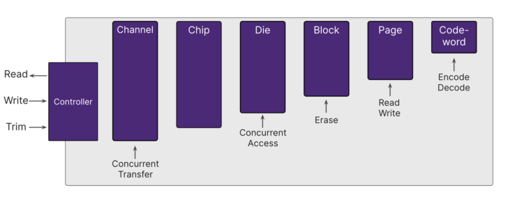
The closest analog to our block on a spinning disk would be the page in NAND flash, which can be tens of kilobytes. A page can be read, and if empty, it can be written to. However, a group of pages together form a block, and that is the level at which you must erase (these blocks can be tens of megabytes). Thus, the three major operations (read, write, and erase) aren’t all available at the same scope. This means that NAND flash is not byte-addressable in the same way that spinning disks are.
This complexity breaks a lot of assumptions made by filesystems, operating systems, and applications alike. If an operating system is used to reading, writing, and erasing logical 4k blocks at a time, and suddenly it finds out that it can’t overwrite a 4k block and instead has to erase several megabytes to do that, you’re gonna have a bad time.
To solve this problem, engineers turn to a solution commonly used in computer science: Add another layer of indirection. To make the operating system think it’s seeing a hard drive and continue using the semantics it’s used to, the concept of the flash translation layer was born. This layer has many jobs, but the end result of all of them is that to an observer looking at the drive from the outside, it would just appear to be a very fast hard drive and mask any of the underlying complexity of the flash media.
The downside of this is you’ve now added a bunch of complexity inside your SSD, and that layer is now responsible for:
- Tracking where all the logical blocks are actually stored
- Culling and rewriting blocks that have pages in them with “tombstoned” data (bits of data that are no longer referenced by anything (aka garbage collection)
- Tracking the number of erase cycles for every cell to avoid wearing out some flash before others (aka wear leveling)
- And more
All this intelligence takes computing power and memory, and so every individual SSD is really its own independent storage array, complete with controller chips, firmware, DRAM, multiple banks of flash chips, and so on. It also means that to maintain this illusion, the drive itself has to burn program/erase cycles moving data around and also has to keep more actual flash storage than it presents to the system so that you have spare space to work with during these operations.
While this may work great for a single drive, it makes building large systems full of SSDs problematic. How so?
The Traditional Approach
Most flash vendors’ products use SSDs built by flash OEMs. Modern SSDs are indeed engineering marvels, but they’re fundamentally exposed to the system the same way hard drives are—as a contiguous group of LBAs, with no transparency into the underlying flash media. Building a system this way makes it easy to drop flash into an array originally designed for hard drives, but it’s a poor choice for an overall system designed to be all-flash.
Why? Lack of visibility and granular control.
First, there’s an inability to see what’s going on within the drive at a system level. If you want to build an enterprise storage system that uses SSDs, you’re essentially treating every solid-state drive as a black box—you really don’t know what it’s doing at any particular time, except by external examination. Say you wanted to read from that drive, but it’s in the middle of a garbage collection cycle. Tough luck; it’s busy.
Second, drives are isolated and lack context as to what the overall system is doing. A drive doesn’t know what kind of data or requests to expect, so you can’t make smart decisions about when to manage your own media. In that kind of system, the management of spare space, garbage collection, and wear leveling falls on the drive, not the system. Each drive in the system does this same work in isolation from each other.
This lack of visibility and granular control is expressed as long tail latencies on some operations in unpredictable ways. And this will only get worse over time as program cycle times increase as density increases. As data grows linearly, that time grows exponentially. QLC drives today require multi-phase program cycles, where the data is written once, then sampled, and then adjusted after a period of time to ensure proper commitment to the cell.
To sum up: In the long term, ceding flash innovation to a drive OEM means you’re a passenger on their bus, not the driver.
Why Not Add Another Layer of Indirection?
An approach to masking the problems of flash at a system level is to do what the SSDs have done: Add another layer in between your slow QLC drives and the systems accessing it. This approach is similar to how hybrid disk/flash arrays use flash to speed up disk-based arrays, only with disk/flash replaced by QLC flash/some extremely fast media, such as persistent memory technologies such as storage class memory (SCM). This, however, presents the same challenges that those hybrid systems encountered a decade ago: Not all workloads are suitable for caching or tiering strategies, and so no matter what strategy you take, you’ll end up with workloads where your clever engineering falls over.
Just as important, each of these extra layers adds cost, complexity, and power utilization. If your use of QLC drives needs expensive SCM to perform well, your system will be more expensive to build, use more power, and still have workloads where you end up falling back to the speed of commodity QLC drives.
Our Approach: Better Science with DirectFlash
At Pure Storage, we take a different approach. We believe flash should be managed at a system level, not a drive level. We call this DirectFlash®, and it’s the foundation of all our all-flash storage products.
DirectFlash is something that makes Pure Storage unique in the enterprise storage industry. It provides us advantages in three key areas over the traditional approach:
- Efficiency: By eliminating duplicate efforts and processes that happen on every drive in a traditional system, DirectFlash increases the overall media efficiency and DirectFlash lowers costs for our systems. By centralizing the flash translation layer, our DirectFlash Modules don’t require DRAM for storing metadata. Petabyte-scale systems that leverage SSDs can have terabytes of DRAM in the drives themselves—not even including system memory. Each drive also contains its own overprovisioned sparing space (up to an extra 20%) that’s necessary for media management by the FTL in the integrated controller, on top of spare space that the overall system will reserve for itself. Each one of these components is an added cost that over time will make up a larger and larger portion of the overall media cost. In contrast, Pure’s approach delivers efficiency and reduces costs.
- Performance: Visibility to the incoming IO patterns allow us to lay out data across the NAND in more intelligent ways that benefit read performance later on, as well as reducing write amplification. Doing fewer writes benefits performance as the flash spends less time doing its slowest operations (program/erase) so it can spend more time fulfilling client requests. And when it can’t be avoided, page-level visibility means we can prevent unpredictable latency spikes by being aware of when a portion of a drive is busy with a program/erase cycle and schedule around it, even by reconstructing data from parity rather than waiting for that flash die to become available for reads.
- Endurance: Lower write amplification not only benefits performance but also endurance since we use significantly fewer program/erase cycles on our flash media over time. This has a direct impact on flash lifespan. QLC media in particular has significantly lower endurance than prior generations (on the order of 1,000 cycles) and so preserving as many of these as possible is paramount to maintaining drive endurance over the lifetime of a module. And with our phone-home telemetry and Pure1®, we can make adjustments to our media management engine over time through software updates to improve endurance (and performance) even further. As a result, the Annualized Return Rate of our DirectFlash Modules is significantly lower than traditional SSDs.
Simply put, DirectFlash is “better science.” By building our own drives that work in concert with the system itself, we enable smarter decisions based on broader context. Our software can understand the activity of the system from the block, file, or object level all the way down to an individual flash cell. With this, you can maximize efficiency by laying out data in ways optimized for the media, significantly lowering write amplification and increasing endurance. And you avoid duplicate work by centralizing functions like garbage collection, sparing, and wear leveling. DirectFlash is a key philosophy that’s part of what makes our products so great. DirectFlash is also an example of one of our key engineering principles: Do things the right way, not the easy way.
As a companion to this article, we’ve also recorded a podcast which goes into even more depth on not just what DirectFlash is but a lot more of the why and how.
More Better Science
DirectFlash isn’t the only foundational technology that underpins our products. If you want to store quadrillions of bits or petabytes of data, the next obvious question is: How do you find anything in that giant ocean of bits? For the answer to that, read Better Science, Part 2: Maps, Metadata, and the Pyramid.


